咨询与报价
EN
A revolution in information technology is taking place by HDI PCB (High-Density Interconnect PCB) in the Period of AI Servers.
GPUs in AI servers with an astonishing power consumption which up to kilowatts brings a opportunity to get creative in a whole new era, from interconnections to materials, design, and manufacturing.
Let’s view the rethinking how we create boards.
Interconnection Density and precision
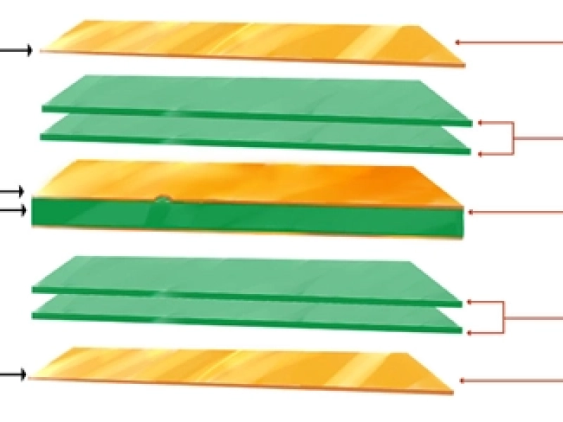
From 4-Step to Any-Layer HDI meets the demands in tighter impedance and denser routing, the pushing motherboard of NVIDIA’s H100 over 20 layers is as symbol of technical challenge.
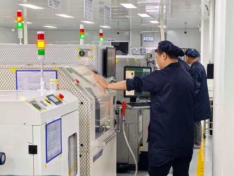
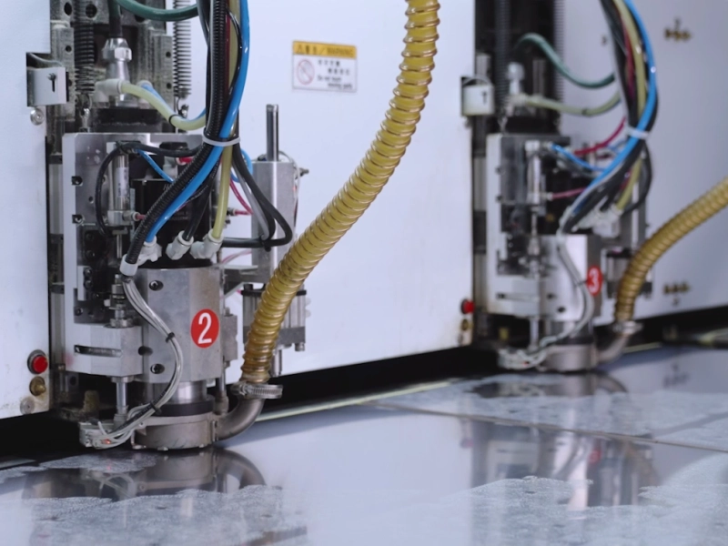
KNOWNPCB have been actually experimenting on exploring multi-layer HDI tech hard, the processing of drilling, LDI imaging, sequential lamination is all part of our toolkit.
1. Stacked microvias: 28-layer, 6-step HDI with 0.8mm staked microvias, routing density up 40% to previous generations.
2. Precision: Any-Layer HDI with ±2 μm precision LDI, which supports complicated AI boards and package.
KNWONPCB does comparable work in High-end GPUs designed in data center, gaming and mid-range, which have a power up to 700 watts to 1000watts.
Remarkable transmission speeds are hitting 112 Gbps PAM4, the speed rate have been applied in wide range of applications, such as advanced packaging solution, 3D printed electronics,5G/6G telecommunications infrastructure.
We have a strong relationship with Panasonic, Isola, Rogers that make sure every AI board with a stable performance in low-loss dielectric and dimension.
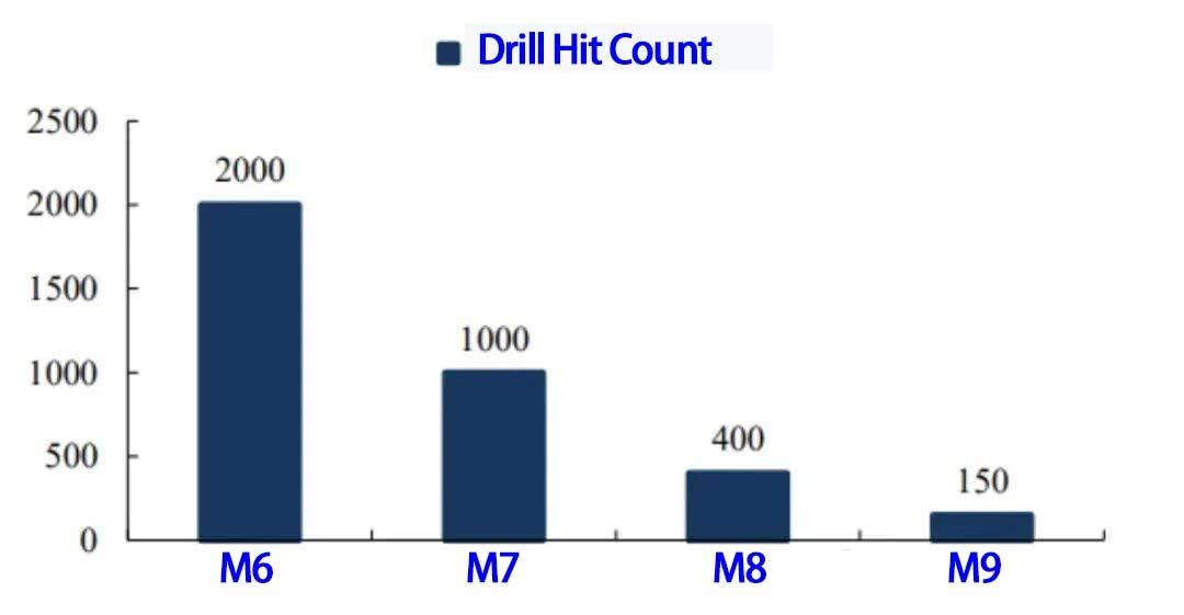
The processing to perform stably after multiple lamination:
It is intense that the heat in GUP areas can get to 150 W/cm². The simulation-driven is designed to a cooler board, cleaner signals.
Precision isn’t simply a buzzword at KNOWNPCB, it is built into the procedure.
The temperature control to ±0.5°C, thickness within 3%
Automated optical alignment with ±8 μm layer registration
Plasma cleaning reducing via roughness to 0.8 μm
KNWONPCB as a China HDI PCB manufacturer with 17-year-experience has been improve the capacity to transform the design requirement in density, precision, cost, quality. KNOWN PCB serves High Density Interconnection PCB to variety of industry, a wide application of smartphones and consumer electronics, which has full size display, ultra-thin form factors, powerful CPUs or GPUs)
As the trends of automotive intelligence and electrification that lead to in-vehicle central control displays, millimeter-wave radar modules, GPS modules, power control units etc required high-performance, highly reliable PCBs. HDI PC board satisfied the demand for an integrated signal and decreased space.
Further introduction about Medical Devices (Endoscopes, portable ultrasound devices, cardiac monitors, high-tech imaging equipment (e.g., modules in CT and MRI machines) , High-Performance Computing & Communication Equipment (Data center servers, high-speed network routers, 5G base station antenna units (AAU), optical modules), please contact us to require case study or PCB type.
Request for a tech support
 | 下载我们的设计指南为了更好的PCB设计和制造 这些是设计师和工程师下载次数最多的设计指南:
|
经7个行业、4000多个客户项目验证
请通过 sales@knownpcb.com 联系我们,或在此处申请工程支持,或使用下方表格联系 KnownPCB。 | 立即咨询 |