咨询与报价
EN
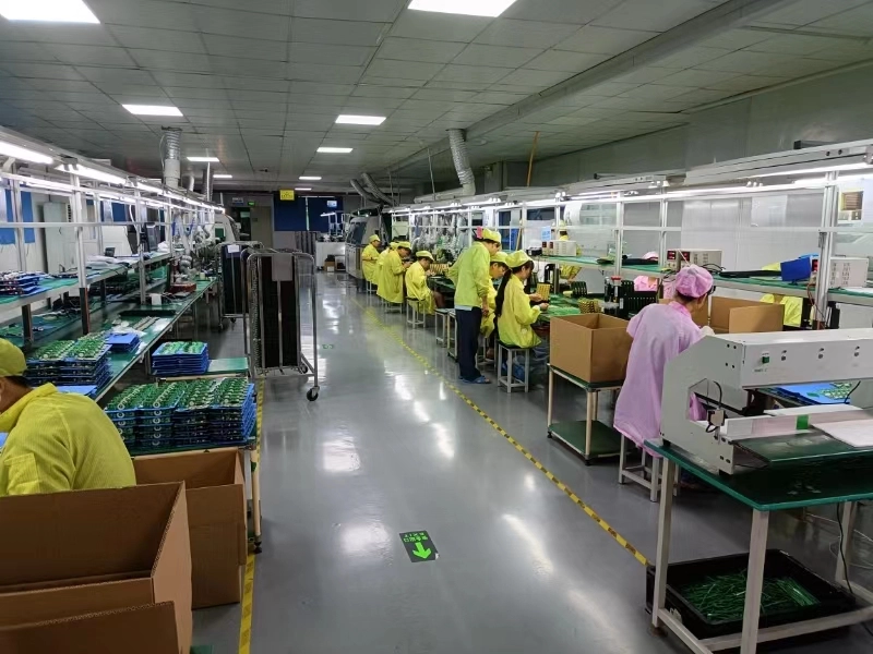
In modern printed circuit board assembly (PCBA), both Surface Mount Technology (SMT) and DIP insertion (commonly categorized as Through-Hole Technology, THT) are widely used in PCB assembly manufacturing to integrate electronic components onto a PCB.
While SMT dominates high-density multilayer PCB fabrication and automated production, DIP remains essential for through-hole parts that require stronger mechanical anchoring, higher current handling, or improved durability under vibration and stress.
Understanding SMT vs DIP helps engineers optimize cost, yield, and long-term reliability, especially for industrial control, automotive electronics, and other high-reliability applications.
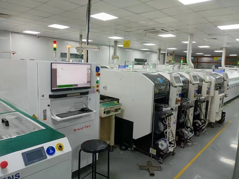
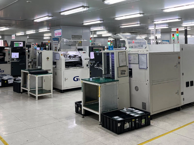
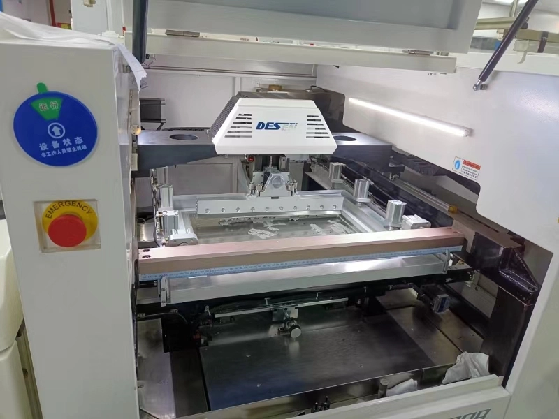
Surface Mount Technology (SMT) mounts components directly onto surface pads using solder paste stencil printing, automated pick-and-place, and a controlled reflow soldering temperature profile. SMT supports compact layouts, higher assembly density, and efficient high-volume production—making it the mainstream option for multilayer PCB assembly and many high-speed digital designs.
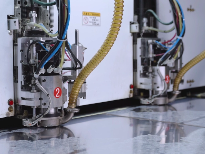
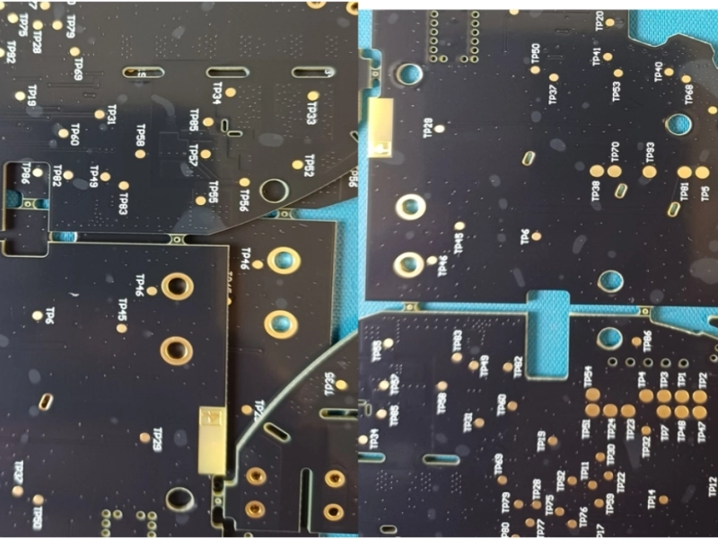
DIP is commonly associated with through-hole technology (THT), where component leads are inserted into plated through holes (PTH) and soldered on the opposite side. Through-hole assembly is often preferred for connectors, transformers, power devices, and parts exposed to mechanical stress or higher current.
| SMT for Printed Circuit Board Assembly | DIP for Printed Circuit Board Assembly | |
|---|---|---|
| specific practice | Solder paste stencil printing + automated pick-and-place mount components onto PCB pads, followed by controlled reflow soldering, AOI inspection, and functional testing. | Insert through-hole components into plated through holes (PTH), then solder via wave soldering or selective soldering. Used for larger, high-current, or mechanically stressed components. |
| main difference | Typically does not require drilling lead holes, enabling higher routing density and faster automated assembly for high-volume PCBA. | Requires drilled and plated holes for leads, providing stronger mechanical retention and improved robustness in vibration or high-power use cases. |
In real-world printed circuit assembly manufacturing, many products use a hybrid SMT + DIP approach to balance density, strength, and cost. The best choice depends on electrical, mechanical, and reliability targets.
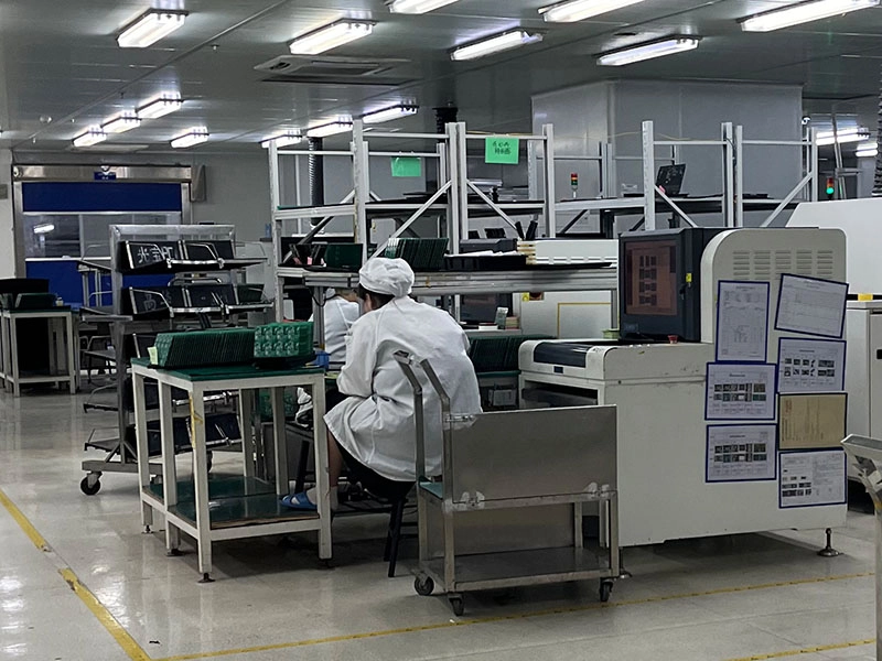
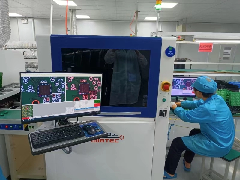
For high-reliability PCBA, stable soldering windows and inspection coverage are critical. Common quality controls include AOI, X-ray inspection (for hidden joints such as BGA), and functional testing. Process control—especially reflow profiling, wave parameters, and material handling—helps improve yield and long-term performance.
Request for a tech support
 | 下载我们的设计指南为了更好的PCB设计和制造 这些是设计师和工程师下载次数最多的设计指南:
|
经7个行业、4000多个客户项目验证
请通过 sales@knownpcb.com 联系我们,或在此处申请工程支持,或使用下方表格联系 KnownPCB。 | 立即咨询 |