咨询与报价
EN
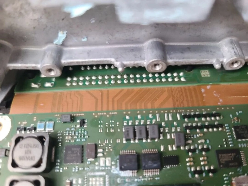
An automotive electronics customer required a compact HDI multilayer PCB for an Advanced driver assistance system (ADAS) camera module which is used in vehicle perception systems. The automotive camera PCB with a CMOS image sensor, processor, and memory is assembled in a very limited circuit boaed area.
The board outline measured approximately 35 mm × 40 mm, leaving minimal routing space for the dense sensor connections and high-speed data signals.
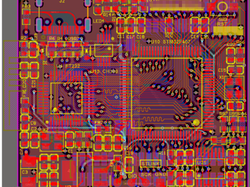
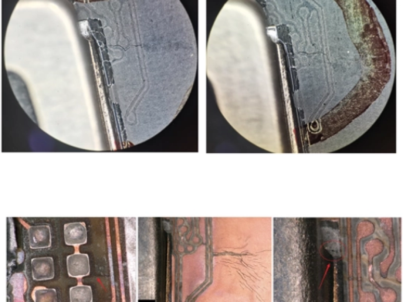
The most critical challenge is the 0.4 mm pitch BGA image sensor, which required reliable fan-out while maintaining controlled impedance for high-speed image transmission. Conventional multilayer routing could not provide sufficient breakout space for the dense BGA pads without increasing the PCB size.
For automotive electronics, reliability requirements are also stringent. The design needed to support stable signal performance while remaining suitable for high-volume automotive PCBA production. Without an optimized HDI structure, dense BGA routing could introduce assembly risks such as solder wicking or bridging during HDI PCB assembly, while impedance discontinuities could affect signal integrity. Over time, these issues may also increase the risk of solder joint fatigue under vibration and thermal cycling in automotive environments.
During DFM review, our engineering team provided recommendations to optimize the 8-layer HDI stack-up to support fan-out of the 0.4 mm pitch BGA image sensor within the limited PCB area.
Laser-drilled microvias (≈100 µm diameter) were used to route signals from the BGA pads to inner routing layers, enabling high-density breakout that would not be possible with conventional through-hole vias. A via-in-pad filled and capped structure was also recommended to maintain flat solderable surfaces and prevent solder wicking during HDI PCB assembly.
In order to support stable signal transmission from the image sensor, controlled impedance routing was maintained across critical signal layers. As an experienced HDI PCB manufacturer, KnownPCB also refined pad geometry and solder mask openings to improve solder joint reliability during automotive PCB assembly.
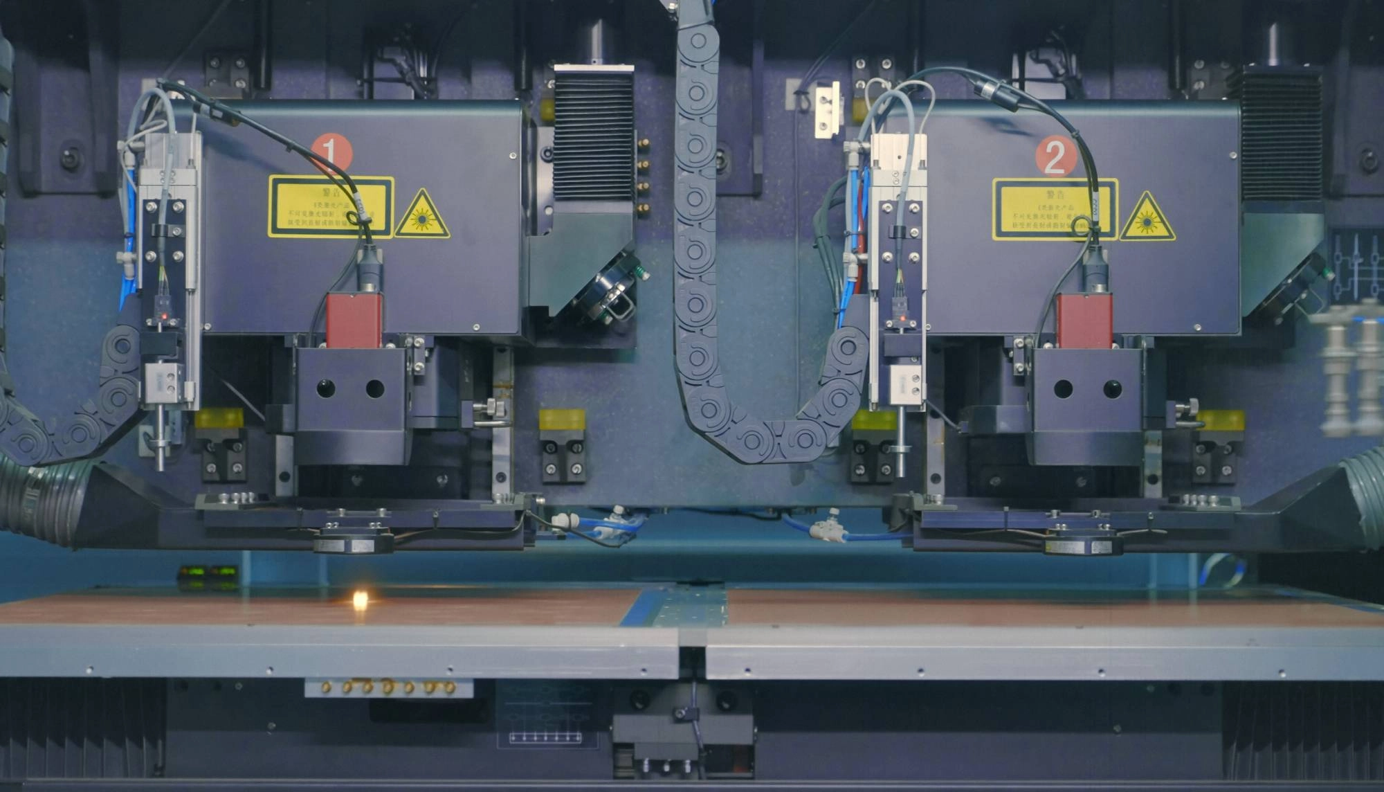
All production was performed under an ISO 9001 certified quality management system, ensuring consistent HDI PCB fabrication and stable printed circuit assembly manufacturing for automotive electronics.
These optimizations enabled reliable fan-out of the image sensor BGA within the original PCB outline while supporting consistent HDI PCB assembly during volume production.
The optimized automotive sensor PCB successfully enabled dense routing of the image sensor without increasing the board size.
After prototype validation, the board entered stable production as part of the ADAS camera module.
Prototype boards were also validated under temperature cycling conditions typical for automotive electronics, confirming stable performance of the HDI PCB structure.
While this project focused on an ADAS camera module, similar HDI solutions are widely used in other automotive sensor PCB and vehicle electronics applications. KnownPCB supports customers developing compact electronic modules that integrate sensors, processors, and memory, providing reliable HDI PCB fabrication, HDI PCB assembly, and automotive PCB assembly for a wide range of automotive electronics systems.