咨询与报价
ENChallenge - The recommended HDI stack-up, such as '2+N+2' or '3+N+3', is to optimize for microstrip antenna integration and stable RF impedance control in mmWave automotive radar applications.
•Solution - DFM review and impedance verification confirmed the stack-up and routing were compatible with HDI PCB fabrication.
•Transition - The HDI multilayer structure supported reliable RF routing without requiring changes to the original PCB layout.
•Result - The radar module PCB moved smoothly from prototype fabrication into stable automotive PCBA production.
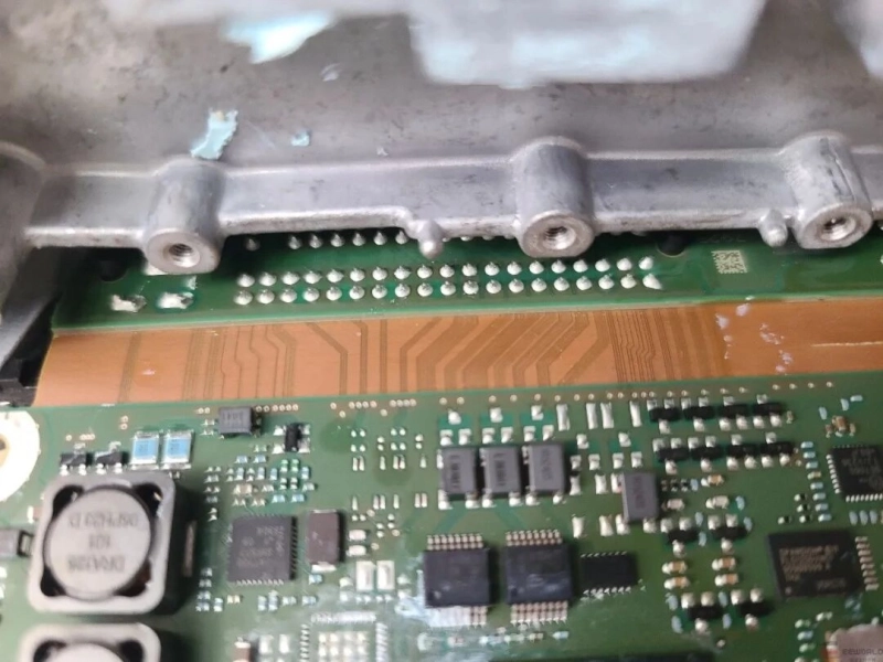
One of KnownPCB customers which is automotive electronics manufacturer was developing a radar sensing module as part of a broader ADAS platform. The internal electronics were applied on a dense HDI multilayer PCB integrating the radar transceiver IC, processor, memory, and supporting power management circuitry within a tightly constrained board outline.
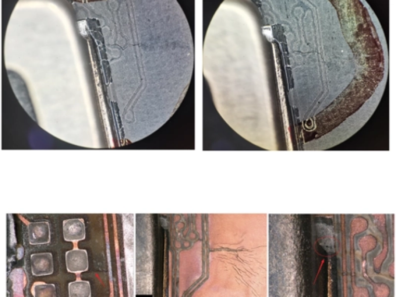
After completing the initial PCB layout, the client's engineering team shared the PCB fabrication data with KnownPCB to review manufacturability before prototype production. During this HDI PCB DFM review, we paid particular attention to the RF routing layers that is used by the radar front-end.
Automotive radar systems operate in the millimeter-wave frequency range , where maintaining stable impedance along RF signal paths is critical for system performance. Manufacturing analysis showed that variations in dielectric thickness, copper profile, and lamination parameters during HDI board fabrication could introduce impedance variation across RF traces. While the design itself met electrical requirements, ensuring consistent RF characteristics across fabrication panels became an important consideration before moving forward with production.
The factors should be involved:
1. Dielectric Material Consistency
2. Copper Profile & Etch Factor
3. Lamination & Registration (Layer-to-Layer Registration, Scaling)
4. Surface Finish Impact: Thickness of immersion silver
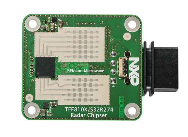
Image source: NXP Semiconductor
Although each design requires its own stack-up configuration, automotive radar PCBs often follow similar manufacturing guidelines to support RF signal integrity.
Parameter Typical Range Layer count 6-10 layers Microvis Type Laser-drilled blind via Via structure Via-in-pad or staggered microvia Lamination process Sequential Lamination Copper thickness 0.5oz-1oz Typical HDI PCB Structure
Parameter Typical Value Dielectric constant (Dk) 3.0-3.7 Dissipation factor (Df) 0.002-0.005 Material Type Low-loss laminate Application frequency mmWave range Typical RF PCB Material Characteristics
Controlled Impedance Targets | |
Signal Type | Target Impedance |
RF signal trace | 50Ω |
Differential signal | 100Ω |
Typical tolerance | ±10% |
Verification method | Impedance test coupon |
Request for a tech support