咨询与报价
EN
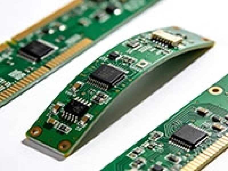
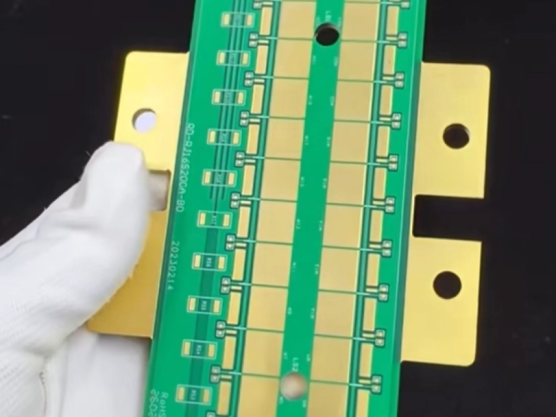
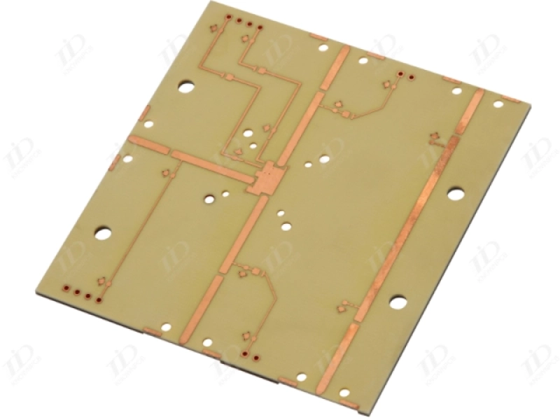
High-density interconnect (HDI) design is widely used in modern electronics that require compact layouts and high routing density. Among various HDI structures, the 4+10+4 stackup presents significant design and manufacturing challenges due to its high layer count, multiple lamination cycles, and complex microvia structures. This article discusses the key challenges in stackup design, material selection, and manufacturing control when producing 4+10+4 HDI printed circuit boards.
HDI technology was first widely adopted in mobile devices, with compact layouts and high routing density required finer traces and laser-drilled microvias. As electronics continued to evolve, HDI PCB is designed for applications such as automotive systems, communication infrastructure, and industrial electronics.
One high-tech circuit board configuration is the 4+10+4 HDI stackup, which consists of 4 build up layers on each side of a 10 layer core. This architecture enables very high routing density but also introduces challenges in stackup planning, material stability, and multilayer PCB fabrication, that requiring precise process control.
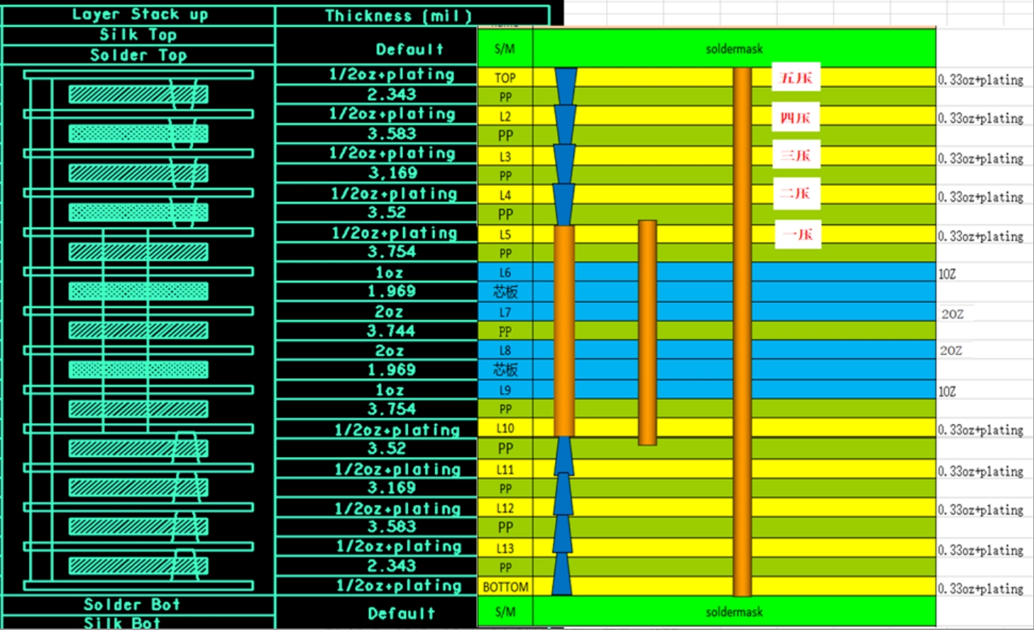
In a 4+10+4 HDI design, in order to maintain impedance consistency and mechanical stability, it's important to carefully control dielectric thickness.
For example:
L7/L8 layers often use two-ply prepreg when routing heavy copper such as 2 oz copper layers.
HDI layout designers should evaluate whether the 10-layer inner core should use three separate core laminates to improve the balance of PCB structure.
HDI circuir board improper core configuration can lead to:
uneven lamination pressure during PCB fabrication
layer shift during PCB pressing
impedance variation in PCB signal layers
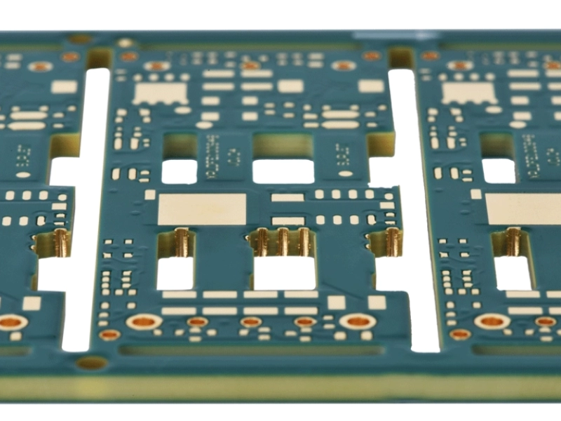
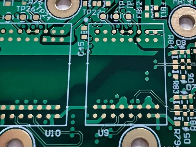
The outer HDI PCB layers usually rely on laser-drilled microvias, typically formed between adjacent layers.
How do layout designers deal with laser drilling quality? For layers such as L6/L7 and L8/L9, layout designers often use 2-mil cores to optimize laser drilling quality and reduce via reliability risks.
However, stacked microvias can increase the risk of PCB quality issues, which are including:
via cracking
incomplete copper filling
interconnect failure during thermal cycling
Thus, in order to reduce these risks, KnownPCB recommend resin-filled vias instead of directly stacked vias, particularly in high-density regions.
Another critical HDI design challenge is maintaining consistent dielectric thickness across multiple layers.
For example, layers such as:
L1/L2
L2/L3
L3/L4
L4/L5
should ideally use similar prepreg thickness whenever possible.
This helps ensure the control of consistent impedance, lamination stress balance and signal integrity improvment.
These challenges of HDI design are particularly important in advanced circuit board designs used in high-speed communication equipments.
A 4+10+4 HDI PCB typically needs multiple lamination cycles, each exposing the material to elevated temperatures and pressure.
Therefore, the laminate material offers:
high Tg (glass transition temperature)
low CTE (coefficient of thermal expansion)
good dimensional stability
If the material cannot withstand repeated lamination, it leads to:
layer misalignment
delamination
increased board warpage
Poor dimensional stability may cause:
misalignment of microvias
registration errors between layers
signal integrity issues
Selecting materials with stable resin systems and controlled glass weave structure is essential for maintaining accuracy in multilayer PCB manufacturing.
Each lamination stage exposes the board to high temperature and pressure, which can affect previously cured layers. Poor control may lead to layer misalignment, internal voids, or delamination.
To improve manufacturability and reliability of an top technology HDI board, hardware engineers should consider the following design guidelines:
Maintain consistent prepreg thickness for signal layers whenever it is possible.
Avoid directly stacked vias in high-stress regions; consider resin-filled vias.
Select laminate materials with high Tg and low CTE to withstand multiple lamination cycles.
Ensure copper distribution is balanced across layers to minimize warpage.
Work closely with an experienced HDI PCB supplier or multilayer PCB manufacturer during the stackup design stage.
These practices can significantly improve yield and reliability in multilayer printed circuit boards which are used in high-performance electronics.
The 4+10+4 HDI PCB architecture represents one of the more advanced multilayer PCB structures that are used in modern electronics. While it offers exceptional routing density and performance benefits, it also introduces significant challenges in stackup design, material selection, and manufacturing control.
By understanding these challenges and collaborating with an experienced HDI PCB supplier specializing in multilayer printed circuit boards fabrication, designers can successfully achieve reliable high-density boards suitable for demanding applications such as communication systems, automotive electronics, and advanced computing platforms.
 | 下载我们的设计指南为了更好的PCB设计和制造 这些是设计师和工程师下载次数最多的设计指南:
|
经7个行业、4000多个客户项目验证
请通过 sales@knownpcb.com 联系我们,或在此处申请工程支持,或使用下方表格联系 KnownPCB。 | 立即咨询 |